_______________________________________________________________________ Special Devices
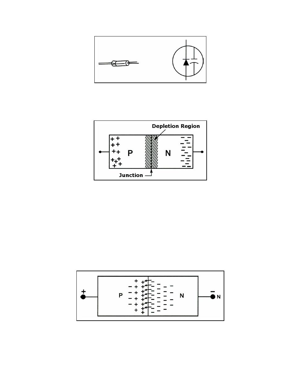
Figure 3-11. Varactor Diode
3-27. Figure 3-12 shows a PN junction. Surrounding the junction of the P and N
materials is a narrow region void of positive and negative charged current carriers. This
area is called the depletion region.
Figure 3-12. PN Junction
3-28. The size of the depletion region in a varactor diode is directly related to the bias.
Forward biasing makes the region smaller by repelling the current carriers toward the PN
junction. If the applied voltage is large enough (about .5 volts for silicon material), the
negative particles will cross the junction and join with the positive particles (see
Figure 3-13). This forward biasing causes the depletion region to decrease, producing a
low resistance at the PN junction and a large current flow across it. This is the condition
for a forward-biased diode. On the other hand, if reverse-bias voltage is applied to the PN
junction, the size of its depletion region increases as the charged particles on both sides
move away from the junction. This condition (see Figure 3-14) produces a high resistance
between the terminals and allows little current flow (only in the microampere range). This
is the operating condition for the varactor diode, which is nothing more than a special PN
junction.
Figure 3-13. Forward-biased PN Junction
23 June 2005
TC 9-62
3-9


 Previous Page
