_______________________________________________________________________ Special Devices
Figure 3-4. Schematic Symbols for Zener Diodes
The Tunnel Diode
3-16. In 1958, Leo Esaki, a Japanese scientist, discovered that if a semiconductor
junction diode were heavily doped with impurities, it would have a region of negative
resistance. The normal junction diode uses semiconductor materials that are lightly doped
with one impurity atom for ten million semiconductor atoms. This low doping level results
in a relatively wide depletion region. Conduction occurs in the normal junction diode only
if the voltage applied to it is large enough to overcome the potential barrier of the junction.
3-17. In the TUNNEL DIODE, the semiconductor materials used in forming a junction
are doped to the extent of one thousand impurity atoms for ten million semiconductor
atoms. This heavy doping produces an extremely narrow depletion zone similar to that in
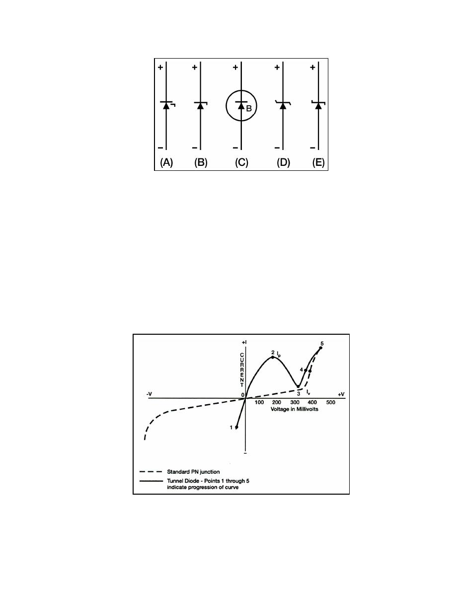
the Zener diode. Because of the heavy doping, a tunnel diode exhibits an unusual current-
voltage characteristic curve as compared with that of an ordinary junction diode.
Figure 3-5 shows the characteristic curve for a tunnel diode.
Figure 3-5. Characteristic Curve of a Tunnel Diode Compared to a
Standard PN Junction
23 June 2005
TC 9-62
3-5


 Previous Page
