_______________________________________________________________________ Special Devices
voltage to control an electrostatic field within the transistor. Since the FET is voltage-
controlled, much like a vacuum tube, it is sometimes called the "solid state vacuum tube."
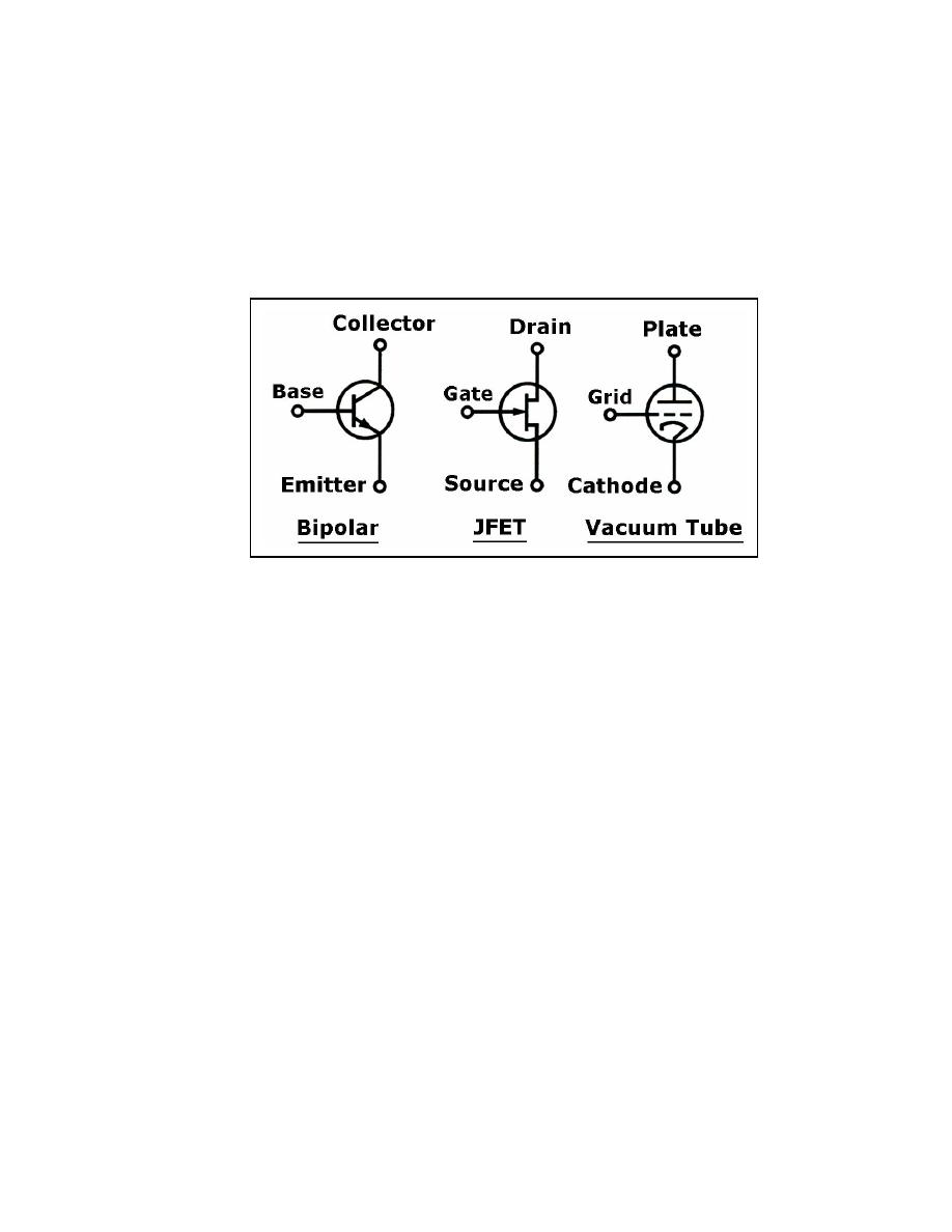
3-74. The elements of one type of FET, the junction field-effect transistor type, are
compared with the bipolar transistor and the vacuum tube (see Figure 3-44). As the figure
shows, the JFET is a three-element device comparable to the other two. The "gate" element
of the JFET corresponds very closely in operation to the base of the transistor and the grid
of the vacuum tube. The "source" and "drain" elements of the JFET correspond to the
emitter and collector of the transistor and to the cathode and plate of the vacuum tube.
Figure 3-44. Comparison of JFET, Transistor, and Vacuum Tube
3-75. Figure 3-45 shows the construction of a JFET. A solid bar, made either of N-type
or P-type material, forms the main body of the device. Diffused into each side of this bar
are two deposits of material of the opposite type from the bar material, which form the
"gate." The portion of the bar between the deposits of gate material is of a smaller cross
section than the rest of the bar and forms a "channel" connecting the source and the drain.
Figure 3-45 also shows a bar of N-type material and a gate of P-type material. Since the
material in the channel is N-type, the device is called an N-channel JFET.
3-76. In a P-channel JFET, the channel is made of P-type material and the gate of
N-type material. Figure 3-46 shows the schematic symbols for the two types of JFET being
compared with those of the NPN and PNP bipolar transistor. Like the bipolar transistor
types, the two types of JFET differ only in the configuration of bias voltages required and
in the direction of the arrow within the symbol. Just as it does in transistor symbols, the
arrow in a JFET symbol always points towards the N-type material. Therefore, the symbol
of the N-channel JFET shows the arrow pointing towards the drain/source channel, while
the P-channel symbol shows the arrow pointing away from the drain/source channel
towards the gate.
3-77. The key to FET operation is the effective cross-sectional area of the channel,
which can be controlled by variations in the voltage applied to the gate. This is
demonstrated in Figures 3-47, 3-48, and 3-49.
23 June 2005
TC 9-62
3-27


 Previous Page
