_______________________________________________________________________ Special Devices
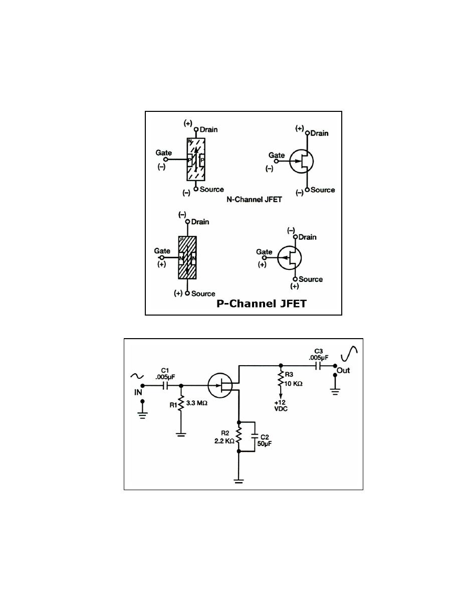
output coupling capacitors. R1 is the gate return resistor and functions much like the grid
return resistor in a vacuum tube circuit. R1 prevents unwanted charge buildup on the gate
by providing a discharge path for C1. R2 and C2 provide source self-bias for the JFET,
which operates like cathode self-bias. R3 is the drain load resistor, which acts like the plate
or collector load resistor.
Figure 3-50. JFET Symbols and Bias Voltages
Figure 3-51. JFET Common Source Amplifier
3-86. The phase shift of 180 degrees between input and output signals are the same as
that of common-cathode vacuum tube circuits and CE transistor circuits. The reason for the
23 June 2005
TC 9-62
3-31


 Previous Page
