TC 9-62
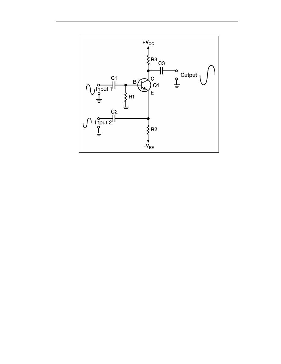
Figure 7-2. Two-input, Single-output, Difference Amplifier
7-14. For the purpose of examining the operation of the circuit in Figure 7-2, assume that
the circuit has a gain of -10. This means that for each 1-volt change in the base-to-emitter
bias, there would be a 10-volt change in the output signal. Also assume that the input
signals will peak at 1-volt levels (+1 volt for the positive peak and -1 volt for the negative
peak). The secret to understanding this circuit (or any transistor amplifier circuit) is to
realize that the collector current is controlled by the base-to-emitter bias. In other words, in
this circuit the output signal (the voltage developed across R3) is determined by the
difference between the voltage on the base and the voltage on the emitter.
7-15. Figure 7-3 shows this two-input, single-output amplifier with input signals that are
equal in amplitude and 180 degrees out of phase. Input number 1 has a positive alternation
when input number 2 has a negative alternation and vice versa.
7-16. The circuit and the input and output signals are shown at the top of the figure. The
lower portion of the figure is a comparison of the input signals and the output signal.
Notice the vertical lines marked "T0" through "T8." These represent "time zero" through
"time eight." In other words, these lines provide a way to examine the two input signals
and the output signal at various instants of time.
7-17. In Figure 7-3 at time zero (T0) both input signals are at 0 volts. The output signal
is also at 0 volts. Between time zero (T0) and time one (T1), input signal number 1 goes
positive and input signal number 2 goes negative. Each of these voltage changes causes an
increase in the base-to-emitter bias, which causes current through Ql to increase. Increased
current through Q1 results in a greater voltage drop across the collector load (R3) that
causes the output signal to go negative.
7-4
TC 9-62
23 June 2005


 Previous Page
