____________________________________________________ Video and Radio Frequency Amplifiers
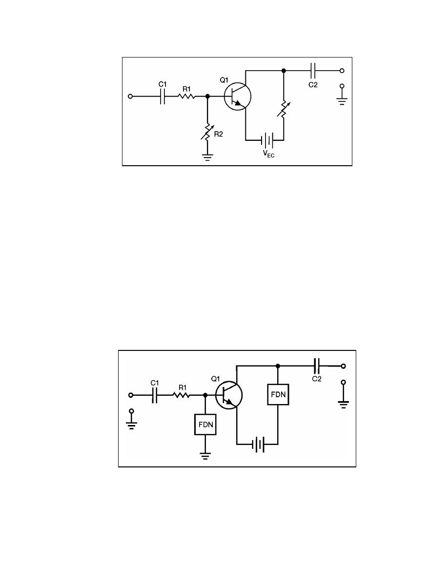
Figure 6-10. Variable Input and Output Impedances
6-45. R1 and R2 form a voltage-divider network for the input signal. When R2 is
increased in value, the input signal to the transistor (Q1) increases. This causes a larger
output signal and the gain of the stage increases. As R3 (output resistor) is increased in
value the output signal increases. This also increases the gain of the stage. As you can see,
increasing the input-signal-developing impedance, the output impedance, or both will
increase the gain of the stage. Of course there are limits to this process. The transistor must
not be overdriven with too high an input signal or distortion will result.
6-46. With this principle in mind, if you could design a circuit that had maximum
impedance at a specific frequency (or band of frequencies), that circuit could be used in an
RF amplifier. This frequency-determining network could be used as the input-signal-
developing impedance, the output impedance, or both. The RF amplifier circuit would then
be as shown in Figure 6-11.
6-47. In this "semi-block" diagram, C1 and C2 are the input and output coupling
capacitors. R1 represents the impedance of the input circuit. The blocks marked FDN
represent the frequency-determining networks. They are used as input signal developing
and output impedances for Q1.
Figure 6-11. Semi-block Diagram of RF Amplifier
FREQUENCY-DETERMINING NETWORK FOR AN RF AMPLIFIER
6-48. A frequency-determining network is a circuit that provides the desired response at
23 June 2005
TC 9-62
6-13


 Previous Page
