_________________________________________________________________ Semiconductor Diodes
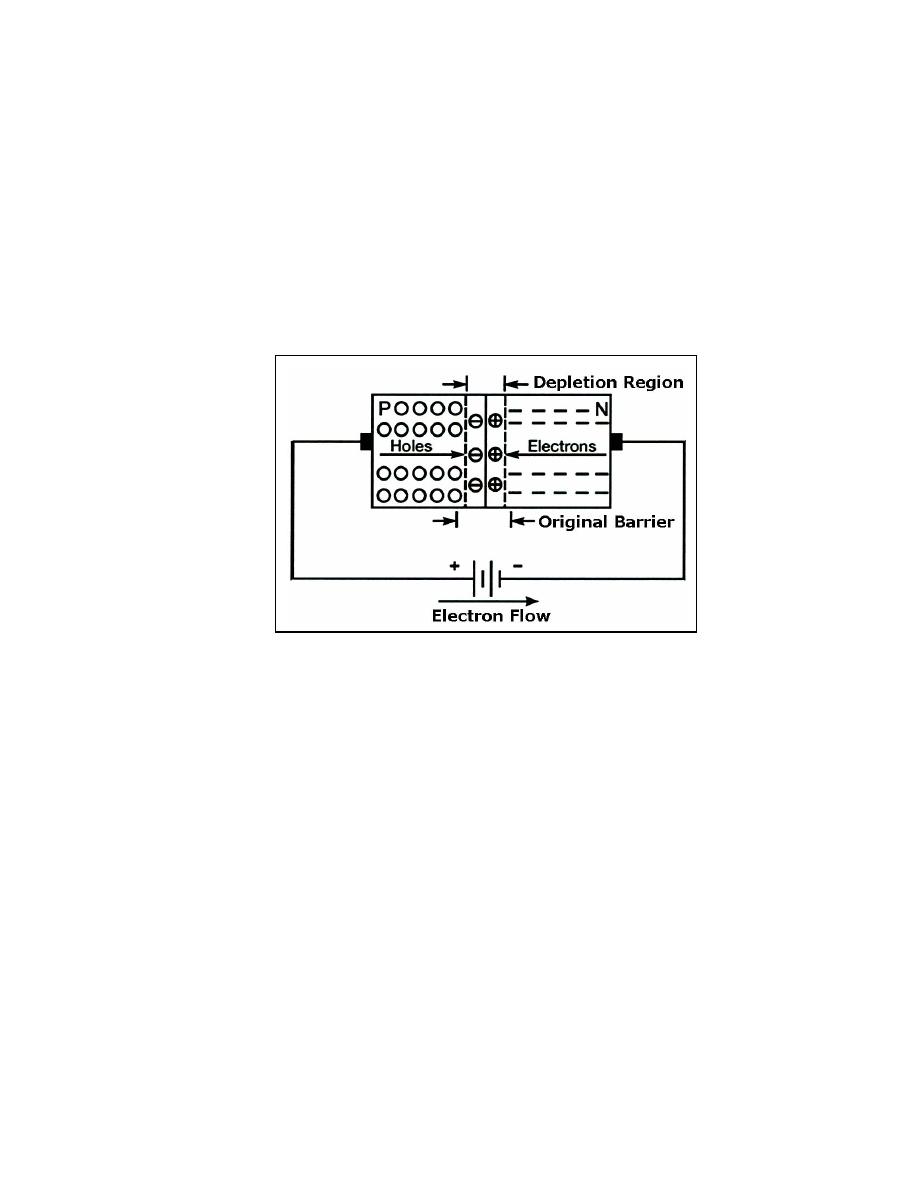
both sides of the barrier are being neutralized, the width of the barrier decreases. So, the
effect of the battery voltage in the forward bias direction is to reduce the barrier potential
across the junction and to allow majority carriers to cross the junction. Current flow in the
forward-biased PN junction is relatively simple. An electron leaves the negative terminal
of the battery and moves to the terminal of the N-type material. It enters the N-type
material, where it is the majority carrier, and moves to the edge of the junction barrier. Due
to forward bias, the barrier offers less opposition to the electron and it will pass through the
depletion region into the P-type material. The electron loses energy in overcoming the
opposition of the junction barrier, and upon entering the P-type material, combines with a
hole. The hole was produced when an electron was extracted from the P-type material by
the positive potential of the battery. The created hole moves through the P-type material
toward the junction where it combines with an electron.
Figure 1-18. Forward-Biased PN Junction
1-72. It is important to remember that in the forward biased condition, conduction is by
MAJORITY current carriers (holes in the P-type material and electrons in the N-type
material). Increasing the battery voltage will increase the number of majority carriers
arriving at the junction and will therefore increase the current flow. If the battery voltage is
increased to the point where the barrier is greatly reduced, a heavy current will flow and
the junction may be damaged from the resulting heat.
1-73. If the battery mentioned earlier is connected across the junction so that its voltage
aids the junction, it will increase the junction barrier and thereby offer a high resistance to
the current flow through the junction. This type of bias is known as REVERSE BIAS.
1-74. To reverse bias a junction diode, the negative battery terminal is connected to the
P-type material and the positive battery terminal to the N-type material (see Figure 1-19).
The negative potential attracts the holes away from the edge of the junction barrier on the P
side, while the positive potential attracts the electrons away from the edge of the barrier on
the N side. This action increases the barrier width because there are more negative ions on
the P side of the junction and more positive ions on the N side of the junction. Notice in
Figure 1-19 that the width of the barrier has increased. This increase in the number of ions
prevents current flow across the junction by majority carriers. However, the current flow
across the barrier is not quite zero because of the minority carriers crossing the junction.
Remember, when the crystal is subjected to an external source of energy (such as light,
heat, and so forth), electron-hole pairs are generated. The electron-hole pairs produce
23 June 2005
TC 9-62
1-21


 Previous Page
