_________________________________________________________________ Semiconductor Diodes
Current Flow in the P-Type Material
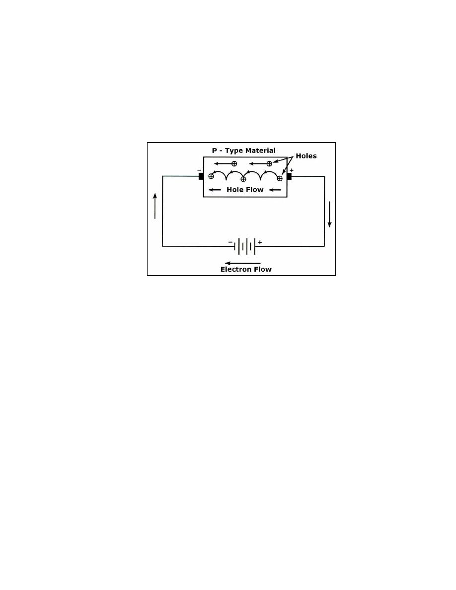
1-63. Figure 1-16 shows the current flow through the P-type material. Conduction in the
P-type material is by positive holes, instead of negative electrons. The hole moves from the
positive terminal of the P-type material to the negative terminal. Electrons from the
external circuit enter the negative terminal of the material and fill holes in the vicinity of
this terminal. At the positive terminal, electrons are removed from the covalent bonds,
thereby creating new holes. This process continues as the steady stream of holes (hole
current) moves toward the negative terminal.
Figure 1-16. Current Flow in the P-Type Material
1-64. Notice in both N-type and P-type materials, current flow in the external circuit
consists of electrons moving out of the negative terminal of the battery and into the
positive terminal of the battery. Hole flow, on the other hand, only exists within the
material itself.
Junction Barrier
1-65. Although the N-type material has an excess of free electrons, it is still electrically
neutral. This is because the donor atoms in the N-type material were left with positive
charges after free electrons became available by covalent bonding (the protons
outnumbered the electrons). Therefore, for every free electron in the N-type material there
is a corresponding positively charged atom to balance it. The end result is that the N-type
material has an overall charge of zero.
1-66. By the same reasoning, the P-type material is also electrically neutral because the
excess of holes in this material is exactly balanced by the number of electrons. Remember
that the holes and electrons are still free to move in the material because they are only
loosely bound to their parent atoms.
1-67. It seems that if we joined the N- and P-type materials together by one of the
processes already mentioned, that all the holes and electrons would pair up. However, this
does not happen. Instead the electrons in the N-type material diffuse (move or spread out)
across the junction into the P-type material and fill some of the holes. At the same time the
holes in the P-type material diffuse across the junction into the N-type material and are
filled by N-type material electrons. This process is called JUNCTION RECOMBINATION
and reduces the number of free electrons and holes in the vicinity of the junction. Since
23 June 2005
TC 9-62
1-19


 Previous Page
