____________________________________________________________________________ Amplifiers
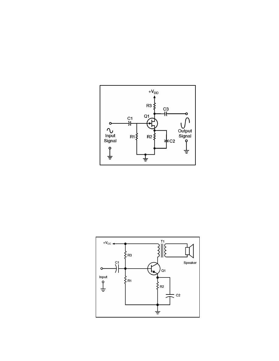
5-82. Figure 5-23 shows the second single-stage audio amplifier. This circuit is a class
A, common-source, RC-coupled, FET, audio amplifier. C1 is a coupling capacitor, which
couples the input signal to the gate of Q1. R1 is used to develop the input signal for the
gate of Q1. R2 is used to bias the source of Q1. C2 is used to decouple the signal
developed by R2 and to keep it from affecting the source of Q1. R3 is the drain load for Q1
and develops the output signal. C3 couples the output signal to the next stage. VDD is the
supply voltage for the drain of Q1. Since this is a common-source configuration, the input
and output signals are 180 out of phase.
Figure 5-23. Class A, Common-source, RC-coupled, FET, Audio Amplifier
5-83. Figure 5-24 shows the third single-stage audio amplifier. This is a class A, CE,
transformer-coupled, transistor, audio amplifier. The output device (speaker) is shown
connected to the secondary winding of the transformer. C1 is a coupling capacitor, which
couple the input signal to the base of Q1. R1 develops the input signal. R2 is used to bias
the emitter of Q1 and provides temperature stability. C2 is a decoupling capacitor for R2.
R3 is used to bias the base of Q1. The primary of T1 is the collector load for Q1 and
develops the output signal. T1 couples the output signal to the speaker and provides
impedance matching between the output impedance of the transistor (medium) and the
impedance of the speaker (low).
Figure 5-24. Class A, CE, Transformer-coupled, Transistor, Audio Amplifier
23 June 2005
TC 9-62
5-23


 Previous Page
