___________________________________________________________________________ Transistors
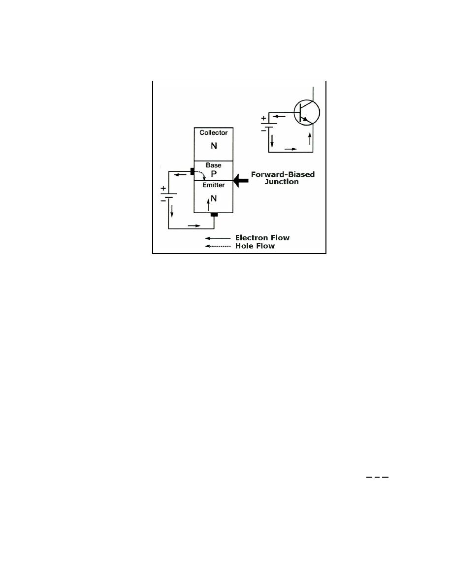
junction (see Figure 2-7) is mainly by majority carrier electrons from the N-type material
(emitter).
Figure 2-7. Forward-biased Junction in an NPN Transistor
2-17. With the emitter-to-base junction in the figure biased in the forward direction,
electrons leave the negative terminal of the battery and enter the N-type material (emitter).
Since electrons are majority current carriers in the N-type material, they pass easily
through the emitter, cross over the junction, and combine with holes in the P-type material
(base). For each electron that fills a hole in the P-type material, another electron will leave
the P-type material (creating a new hole) and enter the positive terminal of the battery.
2-18. NPN REVERSE-BIASED JUNCTION - The second PN junction (base-to-
collector) or reverse-biased junction as it is called (see Figure 2-8), blocks the majority
current carriers from crossing the junction. However, there is a very small current,
mentioned earlier, that does pass through this junction. This current is called minority
current or reverse current. Remember, the electron hole pairs produced this current. The
minority carriers for the reverse-biased PN junction are the electrons in the P-type material
and the holes in the N-type material. These minority carriers actually conduct the current
for the reverse-biased junction when electrons from the P-type material enter the N-type
material, and the holes from the N-type material enter the P-type material. However, the
minority current electrons (as you will see later) play the most important part in the
operation of the NPN transistor.
2-19. You may be wondering why the second PN junction (base-to-collector) is not
forward biased like the first PN junction (emitter-to-base). If both junctions were forward
biased, the electrons would have a tendency to flow from each end section of the N P N
transistor (emitter and collector) to the center P section (base). In essence, we would have
two junction diodes possessing a common base, thereby eliminating any amplification and
defeating the purpose of the transistor. A word of caution, if you should mistakenly bias
the second PN junction in the forward direction. The excessive current could develop
23 June 2005
TC 9-62
2-7


 Previous Page
